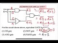
Let's break down this logic circuit step by step to figure out the equivalent gate.
1. First Stage: The inputs $ A $ and $ B $ go into a NAND gate. The output of a NAND gate is the negation of the AND operation. So, the output here is:
$ \overline{A \cdot B} $
2. Second Stage (Top): Input $ B $ also goes into a NOT gate. The output of the NOT gate is the complement of the input, which is:
$ \overline{B} $
3. Third Stage (Top): The outputs from the first and second stages, $ \overline{A \cdot B} $ and $ \overline{B} $, are fed into an AND gate. The output of this AND gate is:
$ (\overline{A \cdot B}) \cdot (\overline{B}) $
4. Second Stage (Bottom): Inputs $ A $ and $ B $ go into an OR gate. The output of an OR gate is:
$ A + B $
5. Third Stage (Bottom): The output of the OR gate, $ A + B $, goes into a NOT gate. The output of this NOT gate is:
$ \overline{A + B} $
6. Final Stage: The outputs from the third stage (top) and the third stage (bottom), $ (\overline{A \cdot B}) \cdot (\overline{B}) $ and $ \overline{A + B} $, are fed into an OR gate. The final output $ Y $ is therefore:
Simplifying the Expression Using Boolean Algebra: Using De Morgan's Laws, we rewrite $ \overline{A \cdot B} $ as $ \overline{A} + \overline{B} $. Substituting this into the expression for $ Y $: